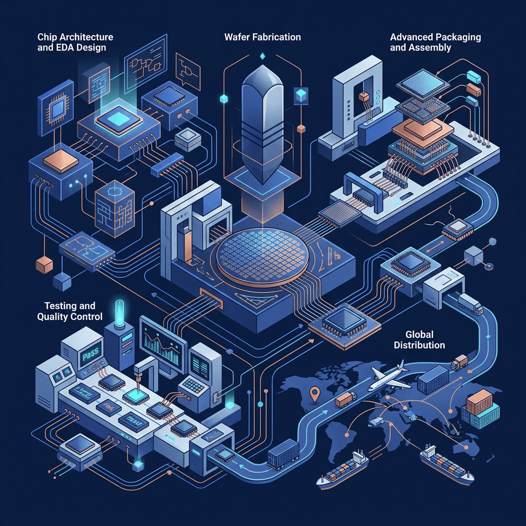
The global semiconductor industry is undergoing a structural transformation that is redefining the parameters of technological sovereignty and economic growth. In 2024, the sector reached approximately $627 billion in sales, a figure that surpassed initial forecasts and set the stage for a record-breaking 2025, where revenue is projected to hit $700.9 billion.[1, 2] This momentum is part of a broader trajectory aimed at reaching the $1 trillion milestone by 2030, with some analysts suggesting the market could expand to $2 trillion by 2040.[2, 3] For entrepreneurs and investors, starting and growing a business in this environment requires a deep understanding of capital intensity, complex manufacturing cycles, and an increasingly fragmented geopolitical landscape.
The primary catalyst for this expansion is the emergence of generative artificial intelligence (gen AI). AI accelerator chips, graphics processing units (GPUs), and specialized neural processing units (NPUs) contributed over $125 billion in sales in 2024 and are forecasted to exceed $150 billion in 2025.[2] However, the industry remains characterized by a high degree of cyclicality, having experienced nine significant contractions over the past 34 years.[3] Successful semiconductor ventures must therefore balance the immediate opportunities in AI with a long-term strategy that accounts for fluctuating demand in automotive, industrial, and consumer segments.
Structural Archetypes: Selecting the Optimal Business Model
A foundational decision for any semiconductor startup is the choice of business model, which dictates the capital requirements, talent needs, and overall risk profile of the venture. The industry has evolved from a vertically integrated monolith into a highly specialized horizontal ecosystem.[4, 5]
The Fabless Innovation Path
The fabless model, pioneered in the 1980s, remains the dominant entry point for design-focused startups. By specializing in chip architecture and outsourcing the capital-intensive manufacturing process to external foundries, fabless firms can focus their resources on research, development, and software-hardware co-design.[4, 6] This model is particularly effective in high-growth markets like AI accelerators, GPUs, and wireless Systems-on-Chip (SoCs), where speed to market and architectural agility are paramount.[5] Companies like NVIDIA and Qualcomm exemplify the success of this model, leveraging external fabrication to scale operations globally with limited fixed assets.[6]
Foundries and the Service-Oriented Manufacturing Layer
Foundries act as the manufacturing backbone of the industry, operating as contract manufacturers that produce chips for fabless firms and Integrated Device Manufacturers (IDMs).[4, 7] This model requires extreme capital investment, with modern fabrication plants (fabs) costing between $10 billion and $20 billion to construct and equip.[5] Pure-play foundries like TSMC dominate this space by driving process node scaling (e.g., 3nm, 2nm) and maintaining high utilization rates.[5] For a startup, entering as a foundry is nearly impossible without massive government backing, but understanding the foundry’s operational constraints is essential for any design-focused firm.
Integrated Device Manufacturers and Vertical Integration
Integrated Device Manufacturers (IDMs) like Intel, Samsung, and Texas Instruments maintain control over the entire value chain, from design to fabrication, packaging, and testing.[5, 6, 8] While this model offers superior control over proprietary process technologies and supply chain resilience, it carries the highest capital risk. Recently, a hybrid IDM model has gained traction, where companies handle critical manufacturing in-house while leveraging external foundries for specific product lines to enhance flexibility and manage costs.[6, 9]
Specialized Ecosystem Roles: OSAT and Design Houses
The backend of the semiconductor process is managed by Outsourced Semiconductor Assembly and Test (OSAT) firms. These specialists provide packaging, assembly, and testing services, which have become increasingly critical as advanced packaging (e.g., 2.5D, 3D stacking) replaces traditional monolithic scaling as a driver of performance.[5, 7, 10] Design Houses serve as another vital layer, acting as a bridge between fabless designers and foundries by optimizing designs for specific manufacturing facilities.[8]
Business Model Comparison for Emerging Ventures
| Business Model | Capital Intensity | Primary Focus | Key Advantage | Target Markets |
|---|---|---|---|---|
| Fabless | Moderate | Design & IP | Agility, Speed to Market | AI, GPUs, Wireless SoCs |
| Foundry | Extreme | Manufacturing | Scale, Technological Moat | All Design Segments |
| IDM | Extreme | End-to-End | Vertical Control, Reliability | Automotive, Memory, Analog |
| OSAT | High | Packaging & Test | Specialized Expertise | High-Performance Compute |
| Design House | Low | Optimization | Connectivity, Ecosystem | Early-stage Startups |
[4, 5, 6, 8]
The Genesis of a Semiconductor Startup: Strategic Planning and Team Assembly
Starting a semiconductor business begins with a rigorous commitment to market research. Entrepreneurs must identify clear customer segments, analyze competitor roadmaps, and uncover specific technological gaps that a new chip architecture can fill.[11] A common pitfall in hardware-driven companies is defining a product without sufficient customer engagement; engineers may assume market needs only to find that hardware changes—which are significantly more expensive than software updates—require 6 to 12 months of redesign and millions in new mask costs.[12]
Assembling the Specialized Team
The human capital requirements for a semiconductor venture are among the most specialized in the technology sector. A core team typically consists of three primary pillars:
- Engineering Architects: Experts in semiconductor physics, circuit design, and process technology responsible for the “idea architecture” of the chip.[11]
- Manufacturing Strategists: Professionals focused on cleanroom protocols, quality control, and yield improvement, ensuring that designs can be reliably produced at scale.[11]
- Sales and Business Development: Individuals who can translate complex technical details into customer benefits and manage the long relationship-building cycles typical of the industry.[11]
Intellectual Property (IP) Strategy
Intellectual property is the primary currency of a semiconductor startup. Protecting innovations through patents is critical for securing a market position and attracting investors.[11] Startups must conduct thorough IP audits to identify valuable assets and gaps in protection early in the R&D process.[13] This strategy often involves filing for patents not just on the product itself, but on novel manufacturing processes and design methodologies.[14] Furthermore, startups are increasingly advised to buy existing IP blocks rather than developing them in-house to reduce time-to-market and upfront investment costs.[12]
The Business Plan and Financial Projections
A semiconductor business plan must account for the extreme upfront costs associated with research, development, and initial fabrication runs. Investors look for a clear prototype or proof of concept that demonstrates market readiness.[11] Financial projections should include both Capital Expenditure (CAPEX) for equipment and land, and Operating Expenditure (OPEX) for raw materials, workforce salaries, and utilities.[15] Given the long development cycles, a startup’s business plan must also outline a robust growth strategy that targets high-value applications like AI servers, autonomous vehicles, or sustainable energy.[11, 16]
The Manufacturing Lifecycle: From Raw Silicon to Packaged Chip
Understanding the physical manufacturing process is essential for any semiconductor professional, as design decisions directly impact the feasibility and cost of production. The journey from raw material to a finished chip involves multiple high-precision stages.[17]
Front-End Processing: Wafer Production and Patterning
The process begins with silicon derived from sand, which is purified and formed into a solid single crystal ingot. This ingot is sliced into thin circular wafers, which serve as the substrate for the circuitry.[17]
- Photolithography: This is the most critical step in defining the chip’s features. A light-sensitive photoresist is applied to the wafer, and ultraviolet light is projected through a mask containing the circuit pattern. Advanced machines like steppers and scanners project these intricate patterns with nanometer precision.[17]
- Etching: Once the pattern is defined, etching machines use chemicals or plasma to carve the circuit patterns into the wafer’s surface, removing unwanted material while the photoresist protects the desired areas.[17]
- Deposition: To build the multiple layers of a chip, thin films of conductive or insulating materials are added using techniques like Chemical Vapor Deposition (CVD) or Physical Vapor Deposition (PVD).[17]
- Ion Implantation (Doping): Impurities are introduced into the silicon to change its electrical properties, a process vital for creating the transistors that form logic circuits.[17]
Back-End Processing: Metrology, Assembly, and Test
Throughout the manufacturing cycle, wafers are inspected using electron microscopes and atomic force microscopes to ensure specs are met—a process known as metrology.[17]
- Assembly and Packaging: Once fabrication is complete, the wafer is cut into individual dies. Each die is tested for functionality before being housed in a protective package that allows it to connect to a circuit board.[7, 17]
- Advanced Packaging Trends: As traditional transistor scaling becomes more difficult, the industry is shifting toward chiplets and 3D stacking. These techniques vertically integrate multiple dies to improve interconnect speed and power efficiency, a market expected to reach $55 billion by 2030.[10, 14, 18]
Manufacturing Process Stages and Equipment
| Stage | Process | Key Equipment | Purpose |
|---|---|---|---|
| Front-End | Photolithography | Steppers, Scanners | Transfer circuit patterns via UV light |
| Front-End | Etching | Plasma Etchers | Carve patterns into silicon surface |
| Front-End | Deposition | CVD/PVD Systems | Apply thin films of metal/insulators |
| Front-End | Ion Implantation | Ion Implanters | Modify electrical conductivity (Doping) |
| Inspection | Metrology | Electron Microscopes | Ensure nanometer-scale precision |
| Back-End | Packaging | Die Bonders, Testers | Protect chip and enable connectivity |
[5, 17]
Navigating the Funding Landscape: Venture Capital and Government Support
Semiconductor ventures require significant initial commitments from specialized investors due to the high costs of equipment, facilities, and skilled labor.[19] However, the current environment is highly favorable for hardware startups, as capital that was once concentrated in software is flowing into the physical infrastructure required to enable AI at scale.[10]
The Venture Capital Ecosystem in 2025
Deep tech already accounts for approximately 20% to 33% of global venture funding as of late 2024.[10] Investors are particularly focused on AI-driven industry transformations, fueling innovation in power electronics, packaging, and next-generation infrastructure.[10]
- Seed and Early-Stage Investors: Firms like Sierra Ventures, True Ventures, and Intel Capital are active in providing the initial capital for semiconductor startups, with “sweet spot” checks ranging from $750,000 to $20 million depending on the firm’s focus.[20]
- Growth and Scaling: As startups reach the early revenue stage, they target larger funds like Accel, Sequoia, and Andreessen Horowitz, which have historically backed some of the world’s largest technology companies.[21, 22]
- Deep Tech Accelerators: Programs like ChipStart in the UK and Silicon Catalyst provide not only mentorship but also no-cost access to design tools and foundry services, significantly lowering the barrier to entry for early-stage innovators.[23]
Sovereign Subsidies and the CHIPS Act
Geopolitical tensions and supply chain vulnerabilities have prompted governments to launch massive incentive programs to secure domestic semiconductor capacity.
- The U.S. CHIPS and Science Act: Signed in 2022, this legislation provides $52.7 billion in federal funding, including $39 billion for manufacturing incentives and $13.7 billion for R&D and workforce development.[24, 25] A key benefit for businesses is the 25% investment tax credit for capital expenses related to establishing or upgrading semiconductor facilities.[26, 27]
- European Ambitions: The EU is targeting a 20% global market share by 2030, supported by programs like the AI Factory initiative and the European Network of Chips Competence Centres.[28, 29]
- India’s Mission: The India Semiconductor Mission (ISM) offers an ambitious 50% federal subsidy, complemented by state-level incentives, to build a comprehensive semiconductor ecosystem.[30]
Top Venture Capital Firms for Semiconductor Hardware (2025)
| Rank | Firm Name | Focus Areas | Notable Geographic Reach |
|---|---|---|---|
| 1 | Accel | Technology, Infrastructure | California, Global |
| 2 | General Catalyst | AI, Deep Tech | California, Global |
| 3 | Andreessen Horowitz | AI Infrastructure, Defense | California, USA |
| 6 | NEA | Hardware, Health Tech | California, USA |
| 32 | Khosla Ventures | Deep Tech, Sustainability | California, USA |
| 34 | DCVC | Data Center, AI Hardware | California, USA |
| 89 | True Ventures | Semiconductors, IoT | California, USA |
[21]
Design Ecosystem: EDA Tools and the “Shift Left” Philosophy
Electronic Design Automation (EDA) software is the essential toolkit used to design and verify complex integrated circuits. The market is dominated by three primary vendors: Cadence Design Systems, Synopsys, and Siemens EDA.[31, 32] These companies are currently investing over 30% of their revenue back into R&D to address the increasing complexity of chips that now house over 200 billion transistors.[31, 32]
The Evolution of EDA and AI Integration
In 2025, the EDA industry is focused on an approach known as “Shift Left.” This philosophy moves testing, verification, and validation earlier into the design process, allowing engineers to optimize for system-level performance rather than just basic power and area metrics.[2]
- AI-Enabled Design: Both Cadence and Synopsys have rolled out AI-powered tools that accelerate the layout and verification process, helping human designers manage the trillions of transistors in modern GPUs and AI accelerators.[31, 33]
- Cloud for Startups: To assist early-stage companies, EDA vendors offer cloud-based subscription models. This shifts spending from large, upfront CAPEX for physical servers to a more manageable OPEX model, providing startups with access to enterprise-grade technology on demand.[33, 34]
Comparing EDA Ecosystems for Startups
For a new business, the choice of EDA partner often depends on the specific technical focus of the chip:
- Digital Design Leadership: Synopsys is widely regarded as the leader in digital EDA, offering robust documentation and unified commands across its suite.[35]
- Analog and Mixed-Signal: Cadence is the preferred choice for analog design, offering “Rapid Adoption Kits” and more extensive online training material that is particularly user-friendly for beginners.[35]
- Physical Implementation: While both offer high-end solutions, designers often find Cadence’s digital design tools to be “lighter” and requiring less hands-on involvement, whereas Synopsys tools allow for deeper optimization by experienced power users.[35]
EDA Market and Financial Dynamics (2025)
| Metric | Cadence Design Systems | Synopsys | Market Trend |
|---|---|---|---|
| Expected CAGR | 15-20% | 15-20% | Outpacing overall semi growth |
| Gross Margin | ~85% | ~80% | High profitability for software |
| AI Focus | Intelligent System Design | Silicon Lifecycle Management | Shift toward AI-enabled layout |
| Startup Program | Cloud for Startups | Cloud for Startups | Increasing cloud adoption |
| R&D Spending | ~30% of revenue | ~30% of revenue | Rising due to design complexity |
[31, 33, 36]
Strategic Supply Chain Management and Foundry Negotiation
For fabless startups, the relationship with the foundry is the most critical component of the supply chain. Securing capacity at a leading-edge foundry like TSMC or Samsung requires more than just capital; it requires a strategic partnership.
Securing Foundry Capacity
Startups typically enter the foundry ecosystem through Multi-Project Wafer (MPW) services. These “shuttle” runs allow multiple companies to share a single wafer, reducing the cost of mask sets and providing a secure way to test prototypes.[37, 38]
- Negotiation Tactics: Startups should look for foundries that offer “MPW to production” incentives. GlobalFoundries, for example, provides revitalized education packages and incentives for customers transitioning from initial prototypes to full-scale production.[38]
- Take-or-Pay Contracts: In highly constrained markets, large hyperscalers often use “take-or-pay” contracts to guarantee demand and underwrite the foundry’s operational costs. While startups may not have the volume for such deals, they should be aware that these agreements can lock up leading-edge capacity for years.[39]
Diversification and Resilience
Growing a semiconductor business in 2025 requires a proactive approach to supply chain resilience. Leaders are increasingly focusing on geographical diversity to mitigate risks associated with regional conflicts and trade tensions.[40]
- Strategic Stockpiling: Maintaining buffer inventories of essential raw materials and components can protect against sudden disruptions.[11]
- Vertical Thinking: Instead of selling only chips, startups might consider selling entire modules or end-products. This “vertical” approach can yield higher profit margins and provide more direct access to customers.[12]
Typical ASIC Pricing Parameters for Calculation
| Parameter | Type of Data | Impact on Total Unit Price |
|---|---|---|
| Dies Per Wafer | Physical Metric | Directly inversely proportional to price |
| Wafer Cost | Fixed Input | Base for all subsequent calculations |
| Wafer Sort Yield | Efficiency Metric | Determines how many usable chips proceed |
| Assembly Cost | Packaging Input | Varies significantly by package complexity |
| Final Test Yield | Quality Metric | Final filter for salable product |
| Test Time | Operational Metric | Influenced by complexity of test protocols |
[12]
Intellectual Property Protection: Strategy and Enforcement
As a semiconductor venture grows, its IP portfolio must evolve from simple patent filings into a sophisticated defensive and offensive strategy. In the advanced packaging domain alone, patent filing has grown at a 12-15% CAGR over the last decade.[14]
Core IP Protection Strategies
A comprehensive strategy involves multiple layers of legal and technical protection:
- Patents: These protect the functional aspects of an invention. Startups should focus on filing patents for their “distinctive differentiators” early in the research process.[13, 14]
- Trade Secrets: Critical for protecting manufacturing formulas and customer lists. These are protected through strict internal protocols and non-disclosure agreements (NDAs).[13, 41]
- Freedom-to-Operate (FTO) Analysis: Before finalizing a product design, companies must perform extensive FTO searches to ensure they are not infringing on existing patents, thereby avoiding expensive litigation.[14]
Licensing and Monetization
Licensing can be a powerful tool for a growing business to unlock value. By licensing out unused IP assets or entering into cross-licensing agreements with competitors, a company can generate recurring revenue and reduce market friction.[14, 42]
- Strategic Alliances: Startups are increasingly entering joint development agreements with academic institutions like imec or Fraunhofer to create foundational IP assets that can be commercialized globally.[14]
- Compliance and Audits: Ensuring that licensees accurately report sales and royalty payments is essential for monetization. Emerging trends include using AI-powered audits to flag reporting discrepancies automatically.[42]
IP Asset Types and Protective Mechanisms
| IP Type | Protective Mechanism | Duration of Protection | Critical Use Case |
|---|---|---|---|
| Patents | Legal Registration | 20 Years from Filing | Novel chip architectures |
| Trade Secrets | Confideniality/NDAs | Perpetual (if kept secret) | Proprietary chemical etching formulas |
| Trademarks | Branding Registration | Indefinite (via renewals) | Company logos and product names |
| Copyrights | Registration/Automatic | Life + 70 Years | Software code and UI design |
| FTO Analysis | Investigative Search | Strategic Action | Avoiding patent infringement lawsuits |
[13, 14, 43]
Geopolitics and the Regulatory Environment of 2025
The semiconductor industry is no longer just a commercial market; it is a matter of national security. Businesses must navigate a thicket of export controls, tariffs, and localization pressures.
U.S. Export Controls and the AI Diffusion Rule
In early 2025, the U.S. Department of Commerce significantly expanded export controls to curtail access to advanced chips by geopolitical rivals.
- Framework for AI Diffusion: This rule imposes global licensing requirements for the most advanced computing integrated circuits (ICs) and the equipment necessary to produce them.[44, 45]
- Tiered Country Structure: The rule establishes three country groups: Whitelisted (Group 1), which includes the U.S. and 18 allied nations; Prohibited (Group 2); and intermediate destinations (Group 3) that require conditional licenses for specific performance thresholds.[45]
- Tariff Impacts: Rising tariffs are contributing to inflationary pressures and forcing companies to sacrifice margins. U.S. tariff revenue from electronics and components expanded from $7 billion in January 2025 to $29.5 billion by August.[30]
Localization and Supply Chain Sovereignty
Governments are pushing for “supply-chain sovereignty,” encouraging companies to build local manufacturing and R&D facilities. This creates both a challenge and an opportunity for startups.
- Regional Incentives: Strategic opportunities exist in regions like South Korea, which focuses on memory leadership, and Japan, which is providing massive subsidies to companies like TSMC and Rapidus to build advanced fabs.[30]
- Compliance Infrastructure: Growing companies must invest in legal experts specializing in international trade and export control classifications to avoid legal liabilities.[11]
Key Regulatory Challenges for 2025
| Regulatory Factor | Implementation / Impact | Strategic Response |
|---|---|---|
| Export Control Laws | BIS Interim Final Rule (Jan 2025) | Appoint specialized compliance officer |
| AI Diffusion Rule | Licensing for advanced computing items | Monitor whitelisted vs. prohibited status |
| Section 232 Tariffs | 50% tariffs on key materials | Diversify sourcing to allied nations |
| Data Protection (GDPR/CCPA) | Regulation of data-driven chips | Embed privacy-by-design in chip logic |
| Environmental Regs | Sustainability mandates (SBTi) | Adopt carbon-aware design workflows |
[11, 18, 30, 45]
Regional Ecosystems and Innovation Clusters
Choosing where to headquarter or expand a semiconductor business is increasingly influenced by the strength of local innovation clusters. These clusters provide access to talent, specialized suppliers, and venture capital.
Top Global Innovation Clusters (2025)
According to the WIPO Global Innovation Index, the distribution of high-intensity semiconductor activity is concentrated in North America, Europe, and East Asia.[46]
- San Jose–San Francisco: Remains the world’s leading cluster for venture capital deals and patent filings in the U.S..[46, 47]
- Shenzhen–Hong Kong–Guangzhou: Tops the global rankings for PCT patent applications, driven by massive domestic investment in self-reliance.[46, 47]
- Dresden, Germany: Has become Europe’s most important hub for automotive-grade semiconductors, especially with the advancement of TSMC’s new fab.[29, 48]
- Hsinchu, Taiwan: The global heart of leading-edge fabrication, housing the most advanced nodes in the world.[29]
Emerging Clusters and Growth Opportunities
Several new cities entered the top 100 innovation clusters in 2025, signaling a broadening of the global ecosystem.
- Bengaluru, India: Ranked as India’s most innovative cluster, benefiting from the national semiconductor mission and a vast pool of design talent.[46, 47]
- Austin, Phoenix, and Miami: These U.S. cities are seeing significant growth in venture activity and advanced manufacturing, supported by favorable state policies and the CHIPS Act.[46, 47]
Innovation Intensity and Top Applicant Profiles
| Global Rank | Cluster Name | Economy | Leading Strength | Top Organization |
|---|---|---|---|---|
| 1 | Shenzhen–HK–GZ | China | PCT Applications | Huawei |
| 2 | Tokyo–Yokohama | Japan | Scientific Publications | Mitsubishi Electric |
| 3 | San Jose–San Francisco | USA | VC Deal Activity | Google/Intel |
| 5 | Seoul | S. Korea | Patent Intensity | Samsung Electronics |
| 21 | Bengaluru | India | Design Talent | Various Design Houses |
| 37 | Austin | USA | VC Deal Volume | Various Startups |
[47]
Future Trajectories: AI, Edge Computing, and Sustainability
As the semiconductor industry races toward 2030, the focus of innovation is shifting toward higher efficiency, local intelligence, and environmental awareness.
The Rise of Edge AI and IoT
While the 2024 AI boom was centered on data centers, 2025 and 2026 will be the “inflection point” for Edge AI. This involves embedding AI capabilities directly into sensors and edge devices, allowing for real-time decision-making without the latency of cloud processing.[18, 49]
- Open ISAs like RISC-V: Startups are increasingly utilizing open-source architectures like RISC-V for IoT and edge devices to reduce licensing costs and increase customization.[6, 18]
- Niche Market Applications: Innovation is rapid in biosensors for healthcare, smart home automation via digital twins, and energy-efficient sensors for the “sustainable IoT” market.[23, 49]
Power Semiconductors and Green Energy
The transition to electric vehicles (EVs) and renewable energy is driving massive demand for power semiconductors made from Silicon Carbide (SiC) and Gallium Nitride (GaN).[16, 49]
- SiC Diversification: Once primarily an automotive technology, SiC is expanding into data centers and industrial power supplies due to its superior thermal management.[16]
- Carbon-Aware Design: New design workflows now integrate carbon metrics, enabling engineers to compare the environmental impact of their chip designs directly within EDA tools like those from Cadence and imec.[18]
Growth Forecasts for Key Market Segments (2025-2027)
| Market Segment | 2025 Projection | 2027 Projection | Growth Driver |
|---|---|---|---|
| Gen AI Chips | $150B+ | Continued Expansion | Data Center/LLM Training |
| HBM (Memory) | $35B | ~$80B | High-bandwidth AI apps |
| SiC Power Semis | Strong Diversification | Mainstream Industrial | EVs and Energy Grid |
| Advanced Packaging | ~10-15% CAGR | Critical Scaling Layer | Heterogeneous Integration |
| IoT Chiplets | Early Pilots | Portfolio Refreshes | Modular Edge AI Design |
[2, 16, 18, 50]
Synthesis and Strategic Conclusions
Starting and growing a business in the semiconductor industry is a pursuit of “hard tech” that requires a sophisticated orchestration of capital, talent, and geopolitical foresight. The path to success is no longer a simple matter of designing the best circuit; it is a multi-dimensional challenge that encompasses the entire lifecycle from raw silicon to system-level integration.
The most critical factor for 2026 is the integration of AI—not just as a product category, but as a design tool and a performance requirement. Ventures that can leverage the “Shift Left” design philosophy and advanced packaging technologies like chiplets will be best positioned to overcome the plateau of traditional Moore’s Law scaling. Simultaneously, the chronic talent shortage and the volatile regulatory environment mean that a successful semiconductor business must be as much a legal and educational enterprise as it is a technical one.
Strategic resilience is found in geographic diversity and supply-chain sovereignty. By aligning with national missions like the CHIPS Act or the India Semiconductor Mission, and by anchoring in high-intensity innovation clusters like San Jose, Dresden, or Bengaluru, startups can secure the resources necessary to survive the industry’s notorious cycles. As the market moves toward $1 trillion and beyond, the architecture of the chip economy will favor those who can balance extreme technical innovation with the pragmatic realities of a physical, regulated, and capital-intensive global supply chain.
——————————————————————————–
- A step-by-step guide to the semiconductor supply chain for investors – The Fifth Person, https://fifthperson.com/step-by-step-guide-semiconductor-supply-chain-investors/
- 2025 Global Semiconductor Industry Outlook | Deloitte US, https://www.deloitte.com/us/en/Industries/tmt/articles/2025-global-semiconductor-industry-outlook.html
- 2025 Global Semiconductor Industry Outlook – Deloitte, https://www.deloitte.com/us/en/insights/industry/technology/technology-media-telecom-outlooks/semiconductor-industry-outlook.html
- What Is A Foundry? The Hidden Hero Of Semiconductor Manufacturing – Rapidus株式会社, https://www.rapidus.inc/en/tech/te0008/
- Semiconductor Business Models – Fab, Foundry, IDM, Fabless & OSAT – SemiconductorX, https://semiconductorx.com/semiconductor-business-models.html
- Semiconductor Business Models: Fabless and Fearless – – DigitalVital HUB, https://digitalvital.org/semiconductor-business-models-fabless-and-fearless/
- Understanding the Semiconductor Value Chain: Key Players & Dynamics | SemiWiki, https://semiwiki.com/forum/threads/understanding-the-semiconductor-value-chain-key-players-dynamics.21125/
- Foundry? Fabless? Learn about the Semiconductor Ecosystem All at Once!, https://semiconductor.samsung.com/news-events/tech-blog/from-foundry-to-fabless-an-overview-of-the-semiconductor-ecosystem/
- Semiconductor Landscape 2025 – Specter Insights, https://insights.tryspecter.com/semiconductor-landscape-2025/
- Looking Past the Hype: Deep Tech Perspectives for 2026 | Celesta Capital, https://www.celesta.vc/insights/looking-past-the-hype-deep-tech-perspectives-for-2026
- How To Start a Semiconductor Business | ClickUp™, https://clickup.com/p/small-business/how-to-start-semiconductor-business
- The 6 Must-Do’s for Semiconductor Fabless Start-ups – AnySilicon, https://anysilicon.com/6-must-dos-fabless-start-ups/
- 10 Essential IP Protection Strategies for Innovators – PatentPC, https://patentpc.com/blog/10-essential-ip-protection-strategies-for-innovators
- Patent Trends & IP Strategy Guide 2025 – Lumenci, https://lumenci.com/blogs/advanced-semiconductor-packaging-ip-strategy-2025/
- Semiconductor Manufacturing Plant Setup Report 2025: Cost Breakdown and Business Blueprint – EIN Presswire, https://www.einpresswire.com/article/830121515/semiconductor-manufacturing-plant-setup-report-2025-cost-breakdown-and-business-blueprint
- Five Key Trends for Power Semiconductors in 2025 | TechInsights, https://www.techinsights.com/blog/five-key-trends-power-semiconductors-2025
- How to Launch a Semiconductor Manufacturing Business in 2025 – IMARC Group, https://www.imarcgroup.com/insight/how-to-launch-a-semiconductor-manufacturing-business
- 6 IoT semiconductor predictions for 2026, https://iot-analytics.com/iot-semiconductor-predictions/
- Deeptech could drive $1T growth in Europe by 2030 | McKinsey, https://www.mckinsey.com/capabilities/business-building/our-insights/europes-deep-tech-engine-could-spur-1-trillion-in-economic-growth
- Top 2025 Semiconductors Seed Investors, https://signal.nfx.com/investor-lists/top-semiconductors-seed-investors
- America’s Top Venture Capital Firms of 2025 – Time Magazine, https://time.com/7309945/top-venture-capital-firms-usa-2025/
- Top Venture Capital Firms in the U.S – 500+ VCs in 2025, https://vc-mapping.gilion.com/venture-capital-firms/united-states
- Government backs next wave of semiconductor start-ups to scale up …, https://www.gov.uk/government/news/government-backs-next-wave-of-semiconductor-start-ups-to-scale-up-growth
- CHIPS and Science | NSF – U.S. National Science Foundation, https://www.nsf.gov/chips
- Semiconductors and the CHIPS Act: The Global Context | Congress.gov, https://www.congress.gov/crs-product/R47558
- The CHIPS Act already puts America first. Scrapping it would poison the well for US investment. | PIIE, https://www.piie.com/blogs/realtime-economics/2025/chips-act-already-puts-america-first-scrapping-it-would-poison-well
- How Does the CHIPS and Science Act Impact Your Semiconductor or Manufacturing Facility? – Angstrom Technology, https://angstromtechnology.com/chips-science-act/
- Semiconductors’ future: Big growth, global risks – PwC, https://www.pwc.com/gx/en/issues/c-suite-insights/the-leadership-agenda/semiconductors-future-big-growth-global-risks.html
- The Most Important Semiconductor Events of 2025 — And What They Mean for Europe and Czechia, https://czechsemiconductorcentre.cz/the-most-important-semiconductor-events-of-2025-and-what-they-mean-for-europe-and-czechia/
- Navigating Geopolitical Shifts and AI-Driven Growth: Insights from …, https://www.semi.org/en/blogs/navigating-geopolitical-shifts-and-ai-driven-growth-insights-from-the-semicon-west-2025-market-symposium
- The State Of The EDA Industry In 2024 – Semiconductor Engineering, https://semiengineering.com/the-state-of-the-eda-industry-in-2024/
- Need help understanding Cadence & Other paid suite of software : r/chipdesign – Reddit, https://www.reddit.com/r/chipdesign/comments/1l4u9o5/need_help_understanding_cadence_other_paid_suite/
- Cadence Vs Synopsys Stock, Which Is Best? – Financhill, https://financhill.com/blog/investing/cadence-vs-synopsys-stock
- Best Cloud Services for Startups: Top Picks & Guide 2025 – Cortavo, https://cortavo.com/cortavo-guides/cloud-services-for-startups
- Is Synopsys more user friendly to beginners compared to Cadence? : r/chipdesign – Reddit, https://www.reddit.com/r/chipdesign/comments/1ica16y/is_synopsys_more_user_friendly_to_beginners/
- How Synopsys and Cadence are fueling the semiconductor industry’s growth engine, https://www.wing.vc/content/how-synopsys-and-cadence-are-fueling-the-semiconductor-industrys-growth-engine
- MPW Service | Foundry | Samsung Semiconductor Global, https://semiconductor.samsung.com/foundry/manufacturing/mpw-service/
- GlobalShuttle multi-project wafer program – GlobalFoundries, https://gf.com/manufacturing-services/multi-project-wafer-program/
- Why Intel must stay independent, spin out its foundry and rebuild its iconic brand, https://siliconangle.com/2025/02/16/intel-must-stay-independent-spin-foundry-rebuild-iconic-brand/
- KPMG Global Semiconductor Industry Outlook 2025, https://kpmg.com/kpmg-us/content/dam/kpmg/pdf/2025/global-semiconductor-industry-outlook-2025.pdf
- Startup Company Best Practices for Protecting Intellectual Property and Trade Secrets, https://www.internetlawyer-blog.com/startup-companys-best-practices-for-protecting-intellectual-property-and-trade-secrets/
- IP License Strategy & Optimization – The Practical Crash Course – Ocean Tomo, https://oceantomo.com/insights/ip-license-strategy-optimization-the-practical-crash-course/
- 5 Essential IP Protection Strategies for Tech Startups – The Rapacke …, https://arapackelaw.com/startups/ip-protection-strategies-startups/
- New U.S. Export Controls on Advanced Computing Items and Artificial Intelligence Model Weights: Seven Key Takeaways – Sidley Austin LLP, https://www.sidley.com/en/insights/newsupdates/2025/01/new-us-export-controls-on-advanced-computing-items-and-artificial-intelligence-model-weights
- US Department of Commerce Issues Interim Final Rule Designed to Protect American AI, https://www.mayerbrown.com/en/insights/publications/2025/01/us-department-of-commerce-issues-interim-final-rule-designed-to-protect-american-ai
- Innovation Cluster Ranking 2025 – WIPO, https://www.wipo.int/en/web/global-innovation-index/2025/innovation-clusters
- Cluster ranking – Global Innovation Index 2025 – WIPO, https://www.wipo.int/web-publications/global-innovation-index-2025/en/cluster-ranking.html
- I.S.E.S. EU 2025 | International Semiconductor Executive Summits, https://isesglobal.com/summits/ises-eu-2025/
- Eight semiconductor sector trends for 2025 (and beyond) – The ST Blog – STMicroelectronics, https://blog.st.com/eight-semiconductor-sector-trends/
- AI Chips News Today: Export Rules and 2026 Supply | EBC Financial Group, https://www.ebc.com/forex/ai-chips-news-today-export-rules-and-2026-supply


Leave a comment